This section is about the design of the CPU of the DWMC-16. It will discuss the design of the Control Logic, the ALU and the Registers.
ALU
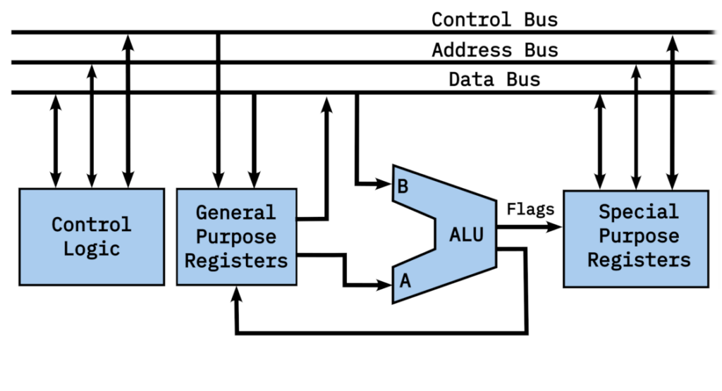
The ALU is one of the core components of the CPU, responsible for computing both arithmetic and logic operations, such as ADD and AND. It is also used to compare two operands for branch operations like BEQ.
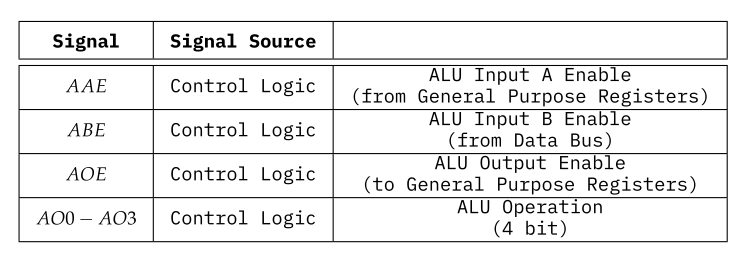
It has two buffered inputs $ A $ and $ B $, as well as a buffered output $ O $, as well as input for control signals to select the operations of the ALU, as well as controlling the input and output buffers.
Input $ A $ is directly connected to only the General Purpose registers, with its buffer D-latch controlled by the $ AAE $ control signal. Input $ B $ is connected to the Data Bus with its buffer D-latch controlled by the $ ABE $ control signal. $ B $ is only connected to the Bus, allowing it to take inputs from memory, as well as from the General Purpose Registers. This allows to reduce the difference between control operations between using inputs to operate on either memory or registers as the second input.
The output $ O $ is directly tied into the General Purpose Registers through ab buffer D-latch controlled by the $ AOE $ control signal. During branch operations, it is not active to transfer the output into the General Purpose Registers, but instead only changes the flags of the Flag Register.
Possible Implementation
Originally it was the intention to design the ALU from scratch, however it was decided that it would be better to simply make use of existing 74 series TTL logic ICs for the ALU. If it is good enough for DEC to use on the PDP-11 and VAX workstation, it is good enough for the \dwmc.
As such the ALU will be utilizing a set of 4 74181 4-bit arithmetic logic unit and function generator in combination with a single 74182 lookahead carry generator. Six 74373 octal latch ICs will be used as input and output latches.
As the 74181 does not support logical shifting of an input, buffer ICs and additional 74194 will be used. Some additional logic will be used to distinguish between shifting and rotating $ A $.
Finally, some logic will have to be used to translate the Control Signals locally to control the 74181, as well as the shift/rotate logic and output buffers.
General Use Registers
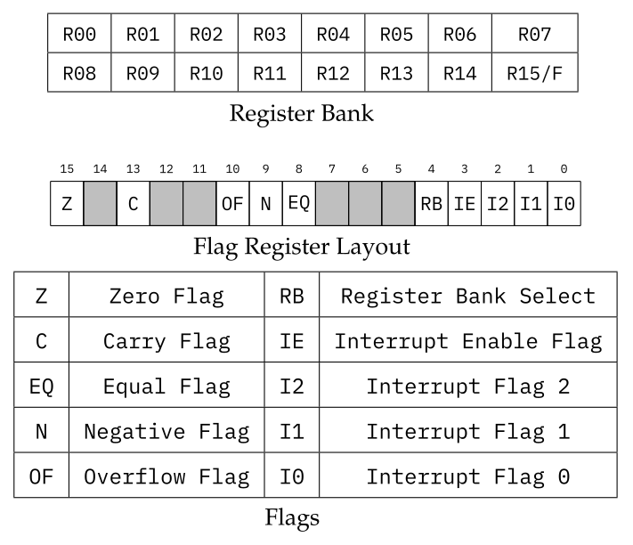
The General Purpose Registers are a set of 16 bit registers, separated into two banks of 16 registers, R00 to R15 and R00' to R15'. They are used to store data internally for quick access by the ALU and the Control Logic.
The ALU or the Data Bus can only access one of the two register banks at a time and to access the other bank it has to be deliberately switched by setting the RB flag in the Flag Register, which sets/resets the $ SELRB $ signal without involving the Control Logic.
Of these registers, R15 and R15' are actually designated the Flag Register F, which can be switched around, but has several signals shared across both Register banks.
The ALU can take inputs from either the Data Bus or the ALU, and output to either the ALU or the Data Bus. The signals $ RRE $, $ RRT $, $ RWE $ and $ RWT $ are used to control the input and output.
Possible Implementation
There are two possible implementations for the General Purpose Registers.
The first implementation is to use eight 74189 64-bit RAM (16×4) ICs in combination with glue logic. However, it is hard to access this time of IC at the time of writing.
The second possible implementation is the use of 74373 octal latch ICs with glue logic, as it is easier to get access to these ICs at time of writing. It will, however, make the PCB for the General Purpose Register Board larger.
For both implementations, three 74373 are to be used for the Flag Register, to enable switching between half of the register, while the second half remains shared across banks.
Special Use Registers
The Special Purpose Registers are a set of different registers that are used for special purposes by the CPU. Other than the General Purpose Registers, they cannot be directly accessed by the ALU or the control logic and are instead accessed via memory access in the memory area between 0x00010 and 0x0001F.
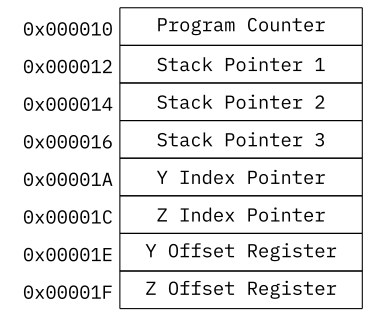
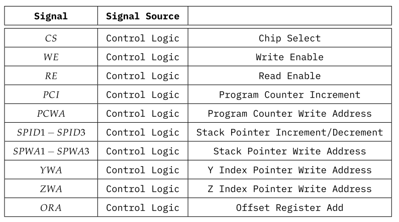
Program Counter The Program Counter is a 20 bit register that contains the current address that is accessed by the CPU. The Program counter can be increased automatically by 1, 2 or 3. It can also be read and written to. Its control signals are $ PCI $, $ PCWA $, $ CS $, $ WE $ and $ RE $. Stack Pointers The Stack Pointers is a 20 bit register that contains the current address of the Systems Stack. That three Stack Pointers are avaiable allows the use of more advanced programming of the system and mplement such things as Task and Interrupt Pointers. The Stack Pointer can be automatically increased and decreased by 1. It can also be read and written to. Its control signals are $ SPID1 – SPID3 $, $ SPWA1 – SPWA3 $, $ CS $, $ WE $ and $ RE $. Index Pointers The Index Pointers are 20 bit registers that contain a memory address that can be used by the CPU for indirect addressing of the main memory. It can be read and written to. Their control signals are $ YWA $, $ ZWA $, $ CS $, $ WE $ and $ RE $. Offset Registers The Offset Registers are 16 bit registers that contain an offset that is automatically added to the corresponding Index Register when the appropriate memory addressing method is selected. Their control signals are $ CS $, $ WE $ and $ RE $. To add to their index registers, the control signal $ ORA $. The selection of the correct Offset Register is done by the $ YWA $ and $ ZWA $ signals.
Possible Implementation
Program Counter Five 74191 synchronous presettable up/down 4-bit binary counter can be used to implement the Program Counter. Stack Counters Five 74191 synchronous presettable up/down 4-bit binary counter can be used to implement the Stack Pointers. Index Pointers Five 74373 octal latches can be used to implement an Index Register. Offset Registers Four 74373 octal latches can be used, in combination with five 74283 4-bit binary full adders can be used, with a single 2:1 multiplexer to select between the adder and the Index Registers.
The Control Logic will be handled in the next post.