Control Logic
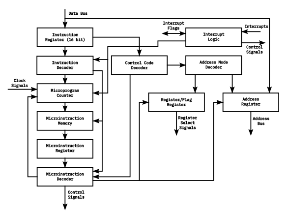
The Control Logic of the DWMC-16 is a microcode based state machine Control Logic, using a reprogrammable microcode instruction memory to save the microcode instructions to save the micro instructions used for the state machine.
Operation
The design Control Logic is heavily based on its operation.
At the beginning of an operation cycle, the Control Logic reads the current instruction from the Data Bus, from the address provided by the Program Counter, saving it to the Instruction Register. From here, it gets split into parts that get decoded by both the Instruction Decoder and the Control Code Decoder.
The Control Code Decoder then pushes the data into Address Mode Decoder, from where the addressing modes of the instruction gets decoded, either saving one or two flags or registers into the Register/Flag Register for use as Register Select Signals, or into the Address Register, which in turn can read from the Data Bus and output to the Address Bus.
The Instruction Decode meanwhile resets the Microprogram counter, which uses a reset-able ring counter to address the Microinstruction Memory, and then provides additional addressing for the Microinstruction Memory, based on the instruction. The selected Microinstruction gets saved into the Microinstruction register.
From here, the Microinstruction is decoded, providing the control signals needed by the CPU and the rest of the computer. At the last microinstruction for a given macroinstructionm the control logic advanced the Program Counter and resets the Microprogram Counter in conjunction with the Instruction Decoder.
It should be possible to combine the Microinstruction Memory, Register and Decoder into a single reprogrammable memory. It should also be possible to integrate the Instruction Decoder into the same memory.
Interrupts
Interrupts are a basic part of the Control Logic and are handled through an integrated Interrupt Logic, which is directly tied into the low byte of the Flag Register.
On receiving an external interrupt from the external control bus, it will decide the Interrupt signal into a 3 bit number, which is pushed into a 3 stage FIFO connected to the $ I0 – I2 $ Flags. After this, the Interrupt Logic waits for the current instruction to be completed, before setting the IE Flag and switching the systems Register Bank to R00' - R15', before saving the Program Counter, Index Registers and Offset Registers to the Stack (possible a dedicated Interrupt Stack).
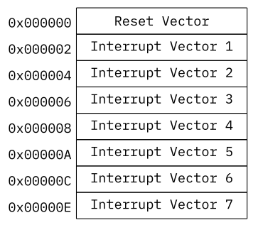
This is followed by selecting one of the Interrupt Vectors from memory, which is written to the Program Counter.
This is followed by the Interrupt Logic waiting until the Interrupt Service Routine is completed and the \texttt{RTI} Instruction returns from the Interrupt. Is the Interrupt FIFO is empty, i.e. no further interrupts need to be handled, the Interrupt Logic writes the Program Counter, Index and Offset registers back from the Stack, allowing the system to return to normal operation.
If another interrupt is in the Interrupt FIFO, the interrupt logic simply writes the new Interrupt Vector to the Program counter and jumps into the new Interrupt Service Routine.
A special Interrupt is the Reset Interrupt, which interrupts the current operation, sets the Program Counter to the address contained in the Reset Vector and resets the Microprogram Counter.
Possible Implementation
The possible implementation of the Control Logic should largely be based around either a set of EPROM, EEPROM or Flash memory ICs, purely based on the possible access time of the ICs in question. The number of ICs is dependent on the number of control signals needed for the system, while the size depends on the number of discrete steps needed for each macroinstriuction. All other components are dependent on other considerations that will come up after the design of the Instruction Set.
Currently one possibility for the memory is using one or more CY27H010, which are available with access times as low as 30ns, though they are likely overkill when it comes to their memory size. Another possibility is the use of the SST39SF010A Flash memory, which is available with 55ns or 70ns access time.
Another possibility would be to use static RAM ICs that are filled with the microcode from an external micro controller on startup. This would also allow to access the micro controller as an IO device to read and write the microcode, allowing the microcode to be modified at runtime from inside the DWMC-16 with a dedicated software package.